CN
CN")
The journey of silicon and its uses– (Author: sunlonge)
More than most industries, ours is identified with a single element, silicon. Silicon wafers are fundamental in manufacturing the electronic “chips” that pervade almost every aspect of our lives. New applications in IoT, wearable and mobile devices, self-driving cars, cloud computing, 5G communication networks, and more, practically guarantee that demand for wafers will continue to grow at an accelerating rate. Construction (sand and concrete) followed by steel and aluminum are by far the largest. There are smaller applications for silicon that are also critical, such as solar energy and specialty parts for semiconductor manufacturing equipment.
Sand to wafers
Fortunately, there is no shortage of raw material. Silicon is the second most common element in the earth’s crust. But silicon does not occur naturally in the pure form needed for electronic applications, for which it must contain less than one in a billion non-silicon atoms. The starting material really is sand. Not just any sand, but silica sand, specially quarried for this purpose and having concentrations of quartz (silicon dioxide) as high as 95%.
")
And more
Silicon is used in many applications other than semiconductor wafers. Ultrapure silicon is also used to make parts for semiconductor manufacturing tools. For example, dielectric etch systems, which remove insulating material used to isolate the conductive components of an integrated circuit, contain critical parts made of high purity silicon. These tools use a process known as reactive ion etching (RIE), which bombards the wafer surface with charged particles (ions) to remove material. The ions are created in a plasma generated by an electromagnetic field applied to a low-pressure gas that is introduced into the process chamber above the wafer. Silicon is an ideal material for critical parts located near the wafer and exposed to the plasma, since it avoids the possibility of contaminating the wafer by redepositing foreign material etched from non-silicon chamber components.
One of the most critical aspects of etch system performance is maintaining the uniformity of the etch process across the wafer, which in turn requires maintaining the uniformity of the plasma. For example, the “showerhead,” through which the etch gas enters the process chamber, contains thousands of holes that must be precisely sized and located to distribute the gas evenly over the wafer. Uniformity can be especially difficult to maintain near the edge of the wafer, where there are electrical, thermal and chemical discontinuities. Surrounding the wafer with an edge ring also made of silicon can significantly reduce these discontinuities. Another critical component best made of silicon is the plasma confinement ring that helps to keep the plasma concentrated over the wafer.
")
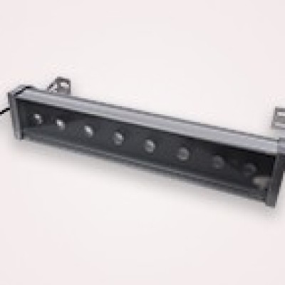
Silicon, which is very hard and brittle, is a challenging material to work with. Silicon wafers, recognizing the criticality and importance to our economy, Sunlonge has invested heavily in developing a reliable solution for the silicon wafer surface inspection. SL8900 wafer inspection lamp is our answer to the semiconductor industry. Due to the high performance, now SL8900 is recognized and accepted by many heavy semi-conductor suppliers in China mainland.