CN
CN

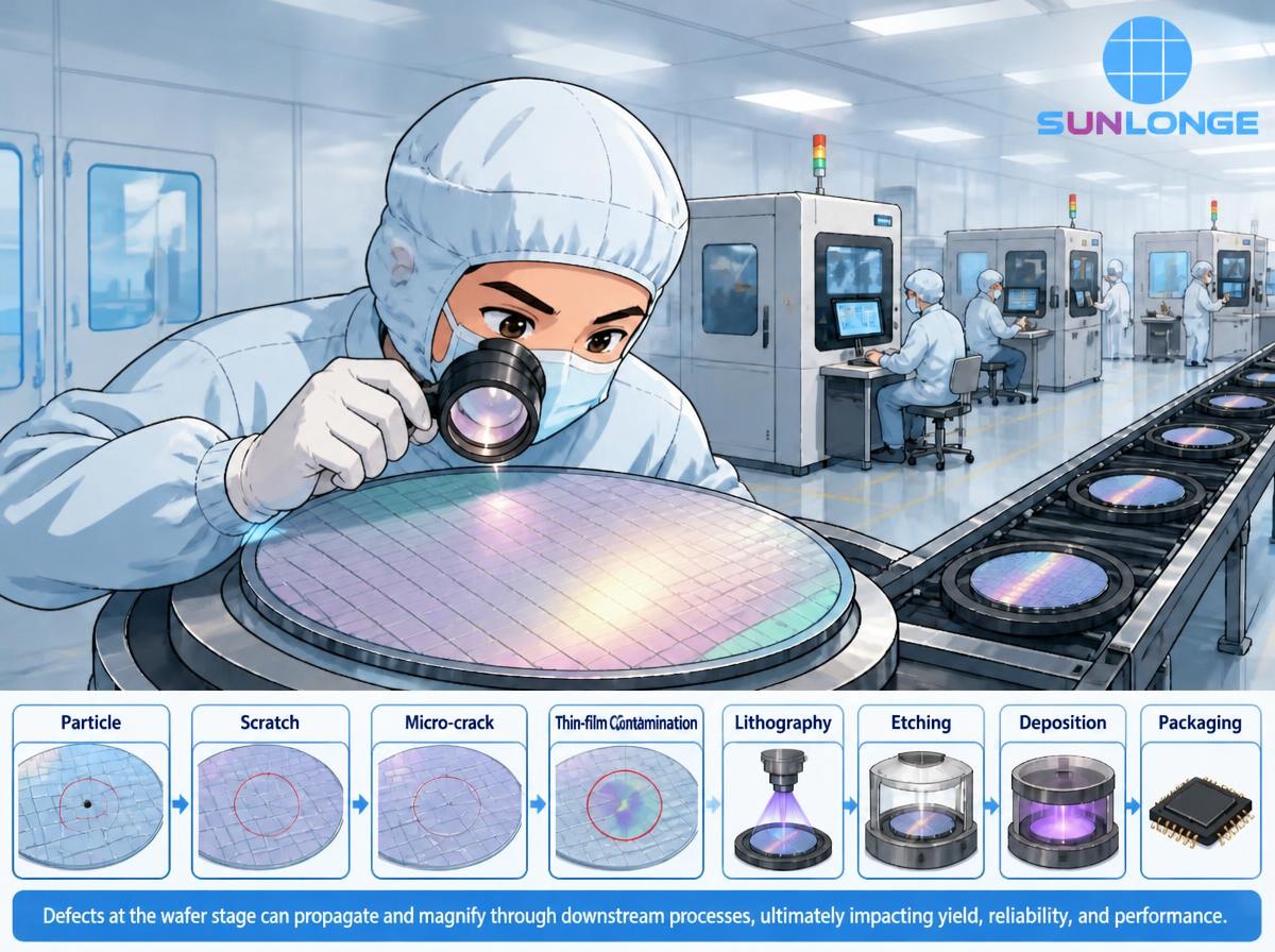
Silicon wafer manufacturing forms the foundation of the global semiconductor industry. Every integrated circuit begins as a highly polished silicon disk whose surface must remain free of microscopic imperfections. Even a single particle, scratch, micro-crack, or thin-film contamination can propagate through lithography, etching, deposition, and packaging steps, ultimately reducing device yield, reliability, and performance. As process nodes shrink toward advanced geometries, the size of critical defects continues to decrease, placing extreme demands on visual and optical inspection.
Standard cleanroom lighting—typically diffuse fluorescent or general LED panels delivering a few hundred to a few thousand lux—is insufficient for reliable detection of these sub-micron and micron-scale anomalies. Specialized wafer inspection lamps solve this problem by delivering intense, wavelength-optimized, highly uniform illumination that maximizes optical contrast between defects and the highly reflective silicon surface. By controlling intensity, spectral content, beam geometry, and viewing angle, these lamps transform nearly invisible surface irregularities into clearly observable features for human inspectors or camera-based systems.
This article examines the optical principles and practical mechanisms by which wafer inspection lamps improve detection of scratches, particles, micro-cracks, and surface contamination. It incorporates industry-relevant performance data and highlights why Sunlonge International’s high-illuminance solutions, particularly the SL8900 series, deliver measurable advantages in semiconductor production environments.
The Challenge of Defect Visibility on Silicon Wafers
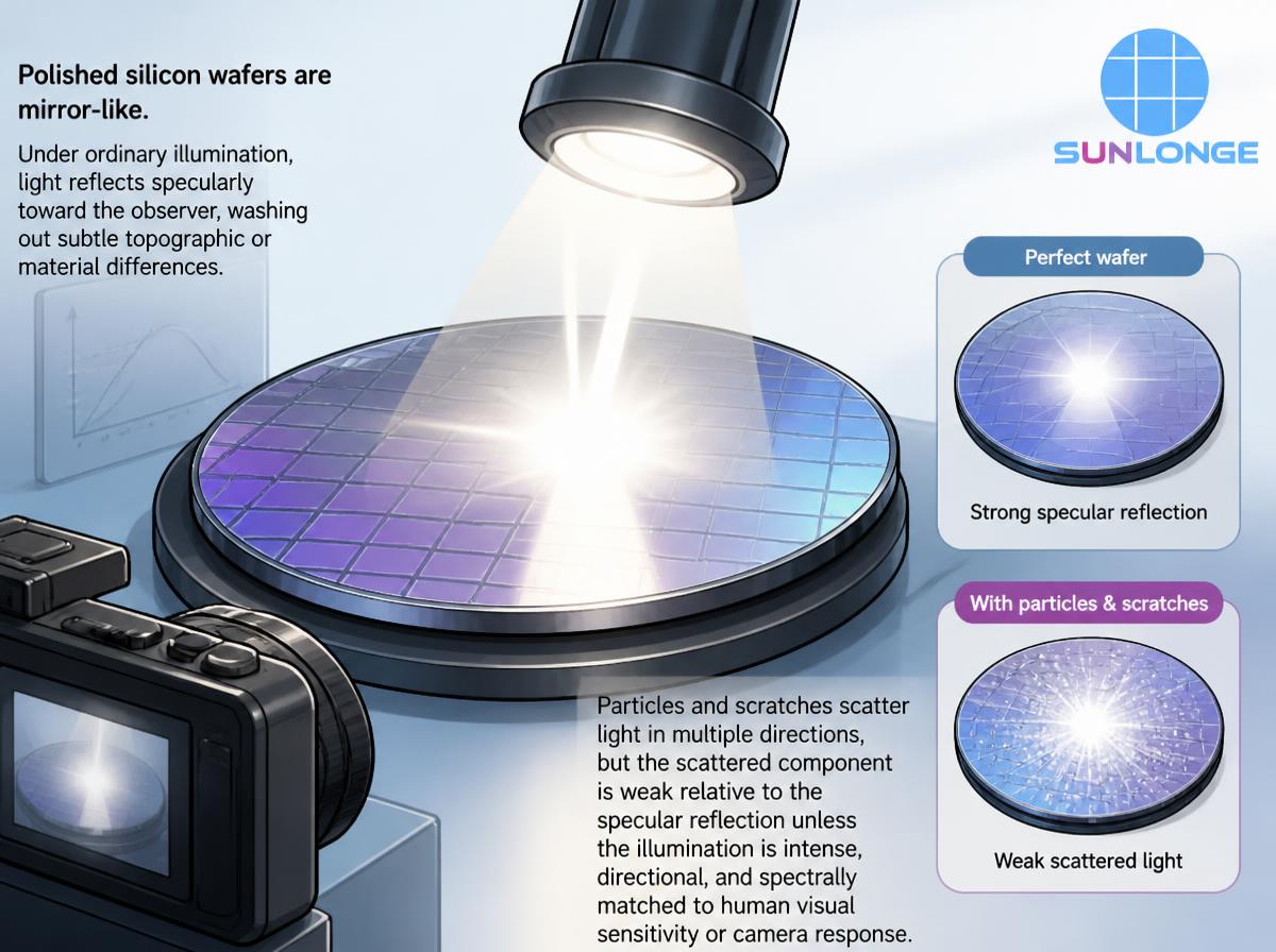
Polished silicon wafers are mirror-like. Under ordinary illumination, light reflects specularly toward the observer, washing out subtle topographic or material differences. Particles and scratches scatter light in multiple directions, but the scattered component is weak relative to the specular reflection unless the illumination is intense, directional, and spectrally matched to human visual sensitivity or camera response.
Industry experience and optical studies consistently show that illuminance levels of 100,000 lux or higher at typical working distances (30–40 cm) are required for reliable naked-eye or low-magnification detection of defects in the 1 µm range. Many traditional inspection lamps fall short of this threshold or suffer from poor uniformity, thermal instability, and short service life. Mercury-vapor sources, once common, generate excessive heat, require frequent replacement, and introduce mercury-handling concerns in cleanroom settings.
A modern wafer inspection lamp addresses these limitations through high-power LEDs, precision optical lenses and filters, mechanical or passive cooling for thermal stability, and selectable wavelengths that enhance specific defect signatures.
Optical Mechanisms That Improve Defect Contrast
Specialized wafer inspection lamps enhance visibility through several interrelated optical effects:
High illuminance increases scatter signal strength. When incident intensity rises, the absolute amount of light scattered by a particle or scratch increases proportionally. At 300,000–400,000 lux, even weak scatterers become bright enough to stand out against the background. Sunlonge’s SL8900 series, for example, delivers 400,000 lux at 30 cm and approximately 280,000 lux at 40 cm using a single 30 W high-power LED with custom optics—performance equivalent to or exceeding a traditional 200 W mercury-vapor source while consuming far less power and generating minimal heat.
Wavelength selection maximizes human visual contrast and material interaction. The human eye is most sensitive in the green-yellow region (approximately 510–590 nm). Green-yellow illumination therefore produces higher perceived contrast for many surface defects. White light (around 6000 K) is effective for coating uniformity and certain contamination layers, while optional narrow bands (365 nm UV, 455 nm blue, 525 nm green, 595 nm yellow, 625 nm red) can be chosen for specific material responses. Sunlonge offers both SL8900-GY (green-yellow) and SL8900-W (white) configurations, plus customizable wavelengths, allowing a single lamp platform to serve multiple process steps.
Controlled beam geometry and dimming optimize the irradiated field. Infinite dimming (0–100 %) combined with adjustable working distance lets operators enlarge or shrink the illuminated area (typically Φ90–200 mm at 40 cm on the SL8900) while maintaining intensity. This flexibility supports both rapid full-wafer overview scanning and focused examination of critical zones.
Oblique or adjustable incidence angles emphasize topography. By tilting the wafer or the lamp relative to the surface, inspectors create low-angle (glancing) illumination. Raised particles and scratch edges scatter light toward the eye while the flat background remains dark—an effect analogous to dark-field microscopy but achievable with a simple desktop lamp and manual manipulation.
These mechanisms collectively raise the signal-to-background ratio so that defects previously lost in specular glare become readily detectable.
Detection Improvements by Defect Type
Particles and dust Airborne or process-generated particles ranging from sub-micron to several microns are among the most common yield killers. Under ordinary lighting they appear as faint spots or remain invisible. High-intensity green-yellow or white illumination from a wafer inspection lamp renders particles as bright points of scatter. Performance claims for advanced lamps such as the SL8900 indicate reliable detection of particles in the 1 µm size range—approximately ten times more effective than conventional lower-intensity inspection lamps. This capability is especially valuable after cleaning, polishing, or transfer steps where residual contamination must be caught before lithography.
Scratches and polishing marks Fine scratches, CMP (chemical-mechanical planarization) swirls, and handling marks scatter light along their length. Green light is particularly effective for slight scratches on silicon and LCD-related surfaces, enabling detection of a high percentage of such defects. The combination of high lux and spectral tuning makes these linear features stand out clearly when the wafer is rotated under the beam.
Micro-cracks and edge defects Micro-cracks and edge chipping produce localized scattering and changes in surface reflectivity. Intense, uniform illumination reveals these discontinuities that standard cleanroom lighting often misses. Early detection prevents crack propagation during subsequent high-temperature or mechanical stress processes.
Surface contamination, residues, and coating non-uniformity Thin films of organic residue, fingerprints, oil, or uneven coatings alter local reflectivity and scatter. White light highlights coating thickness variations and contamination layers, while green-yellow light improves contrast for many particulate and residue types. Operators can switch or select wavelengths to match the dominant contamination mode at a given process stage.
In practice, technicians report that defects invisible under ambient cleanroom lighting become obvious within seconds under a properly adjusted high-illuminance wafer inspection lamp, reducing both miss rates and inspection time.
Quantitative Performance Advantages
Industry comparisons and manufacturer data illustrate the performance gap:
- Typical cleanroom ambient lighting: hundreds to low thousands of lux.
- Traditional inspection lamps: often tens of thousands of lux, with limited uniformity and shorter life.
- Advanced LED wafer inspection lamps: 150,000–400,000 lux at 30 cm, with stability exceeding 90 % and service life of 30,000 hours.
A lamp delivering 400,000 lux at the working distance provides roughly an order-of-magnitude increase in available light compared with many legacy tools, translating directly into higher scatter signal and better detection probability for 1 µm-class defects. LED sources also eliminate the warm-up time, mercury content, and rapid lumen depreciation associated with mercury-vapor lamps. Thermal management keeps surface temperatures low (typically around 50 °C versus 100–150 °C for mercury sources), protecting heat-sensitive wafers and improving operator comfort.
Why Sunlonge Wafer Inspection Lamps Excel
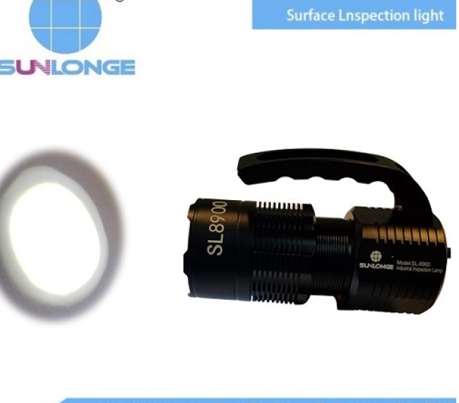
Sunlonge International Co., Limited has developed a focused portfolio of high-illuminance desktop and related inspection lamps specifically for semiconductor, LCD, sapphire, and precision optical applications. The SL8900 series stands out for several technical and practical reasons:
Exceptional illuminance and optical design. A single 30 W imported LED combined with customized optical lenses and filters produces 400,000 lux at 30 cm—among the highest figures published for compact desktop wafer inspection lamps. Uniformity and beam quality are engineered to exceed typical Japanese and German equivalents according to the manufacturer’s comparative claims. Infinite dimming and adjustable irradiated area (Φ90–200 mm class) give operators precise control.
Spectral flexibility and human-visual optimization. Green-yellow (510–590 nm) models align with peak eye sensitivity for maximum contrast. White-light versions and optional discrete wavelengths (including UV and visible bands) allow matching to specific defect or material characteristics. This multi-wavelength capability reduces the need for multiple specialized tools.
Long service life and operational stability. Average LED life of 30,000 hours—approximately ten times that of many mercury-vapor sources—combined with >90 % intensity stability and mechanical cooling ensures consistent performance over years of continuous or high-duty-cycle use. Power consumption remains low (30 W), supporting 24-hour operation from a standard AC supply with DC output regulation.
Practical cleanroom-friendly features. Compact size (approximately 86 × 200 mm, 1.18 kg), low heat output, mercury-free construction, and inclusion of protective glasses make the lamps suitable for direct cleanroom deployment. Battery variants expand flexibility for mobile or intermittent use. Core optical technology enables customization of parallel light characteristics to customer requirements.
Documented detection performance and cost effectiveness. The lamps are specified to detect dust particles and scratches in the 1 µm range, described as roughly ten times more powerful than traditional inspection lamps. By enabling direct visual detection without complex optical systems or microscopes for many macro- and micro-defect classes, they reduce capital and operational costs while improving first-pass yield.
Related models in the Sunlonge range (SL8500, SL8600, SL8100 series) offer graduated intensity levels (150,000–350,000 lux class) so fabs can match performance to process criticality and budget. Collectively these products demonstrate a consistent engineering focus on high illuminance, spectral control, stability, and longevity—attributes that translate into higher defect capture rates and lower total cost of ownership compared with both legacy mercury systems and lower-performance LED alternatives.
Integration into Silicon Wafer Manufacturing Flows
Wafer inspection lamps are typically deployed at multiple process checkpoints: post-polish incoming inspection, after cleaning or CMP, before and after thin-film deposition, edge inspection, and final outgoing quality control. In high-volume fabs they support both manual operator stations and semi-automated setups. The high contrast they provide also benefits camera-based or AI-assisted inspection systems by improving image quality and reducing false negatives.
Because the lamps require minimal infrastructure—standard power, simple mounting, and optional height/angle adjustment—they can be introduced with low disruption and rapid return on investment through reduced scrap and rework.
Comparison Table: Key Performance Metrics
| Parameter | Standard Cleanroom Lighting | Traditional Inspection / Mercury Lamps | Sunlonge SL8900-Class Wafer Inspection Lamp |
| Typical Illuminance (at 30 cm) | 500–few thousand lux | Tens of thousands lux | Up to 400,000 lux |
| Detection Capability (particles/scratches) | Limited; many 1 µm defects missed | Moderate; often > several µm | 1 µm range; ~10× traditional performance |
| Wavelength Options | Broad / fixed white | Limited or broadband | Green-yellow 510–590 nm, white 6000 K, customizable (365–625 nm) |
| Intensity Stability | Moderate | Declines with age | >90 % |
| Service Life | Long for general LEDs | 1,000–few thousand hours (mercury) | 30,000 hours average |
| Heat Generation | Low to moderate | High | Low (cold light source) |
| Power Consumption | Variable | High for equivalent intensity | 30 W |
| Dimming / Beam Control | Limited | Often fixed | Infinite 0–100 %; adjustable irradiated area |
| Cleanroom Compatibility | Good | Mercury handling concerns | Excellent (mercury-free, low heat) |
Figures are representative of published specifications and industry comparisons; actual results depend on exact model, distance, and surface conditions.
Frequently Asked Questions
Q: Why can’t standard cleanroom lighting detect most wafer surface defects? A: Ambient lighting provides insufficient intensity and lacks spectral optimization. Specular reflection from polished silicon overwhelms the weak scatter from particles and scratches, rendering many defects invisible.
Q: What illuminance level is typically required for reliable 1 µm particle detection? A: Practical experience indicates 100,000 lux or higher at the working distance is necessary. Advanced lamps such as the SL8900 reach 400,000 lux at 30 cm, providing substantial margin and improved contrast.
Q: How does green-yellow light improve scratch and particle visibility? A: The 510–590 nm band aligns with peak human visual sensitivity and produces high contrast against silicon surfaces for many topographic and particulate defects. Green light is especially effective for slight scratches; combined green-yellow coverage addresses a broad range of common anomalies.
Q: Can one wafer inspection lamp replace multiple traditional tools? A: High-intensity models with selectable or switchable wavelengths and adjustable beam size often consolidate white-light, green, and yellow inspection tasks into a single compact unit, reducing equipment footprint and cost.
Q: How long do modern LED wafer inspection lamps last compared with mercury sources? A: Quality LED systems are rated around 30,000 hours—roughly ten times the typical life of mercury-vapor lamps—while maintaining high intensity stability and eliminating hazardous-material handling.
Q: Are these lamps suitable for both manual and automated inspection? A: Yes. The high, uniform illumination benefits naked-eye inspection and simultaneously improves image quality for camera or machine-vision systems used in semi-automated or automated stations.
Q: What makes Sunlonge lamps preferable for semiconductor fabs? A: Combination of industry-leading illuminance (up to 400,000 lux), >90 % stability, 30,000-hour life, spectral flexibility, precise optical design, low heat, and proven ability to reveal 1 µm-class defects. Customization of wavelength and beam characteristics further aligns the tools with specific process requirements.
Q: Do these lamps introduce contamination or thermal risk to wafers? A: Properly designed LED systems operate as cold light sources with surface temperatures far lower than mercury lamps, minimizing thermal risk. Mercury-free construction eliminates a potential contamination vector.
Conclusion
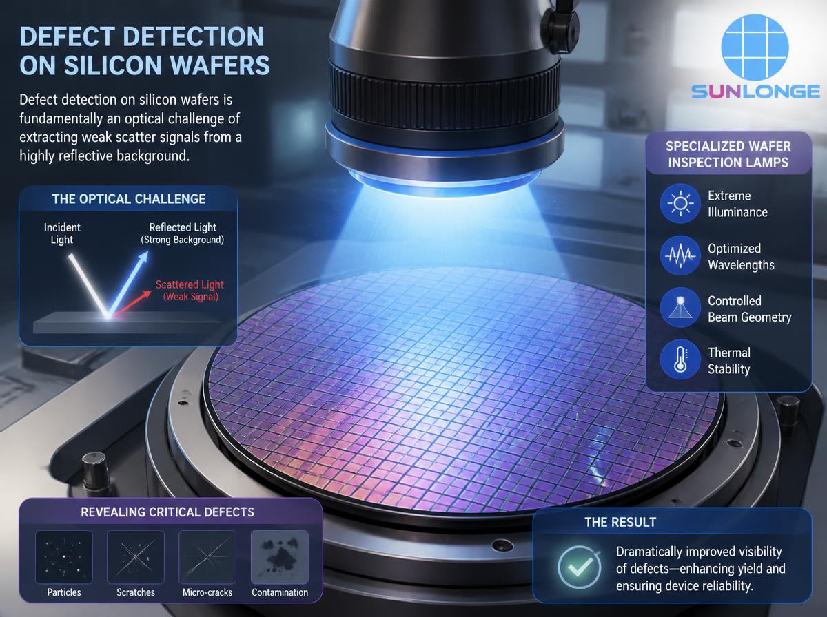
Defect detection on silicon wafers is fundamentally an optical challenge of extracting weak scatter signals from a highly reflective background. Specialized wafer inspection lamps meet this challenge through extreme illuminance, optimized wavelengths, controlled beam geometry, and thermal stability. The result is dramatically improved visibility of particles, scratches, micro-cracks, and contamination—defects that directly influence yield and device reliability.
Sunlonge’s SL8900 series and related high-illuminance models exemplify the current state of the art: 400,000 lux capability, spectral options matched to human vision and material response, long operational life, and practical features tailored to cleanroom semiconductor environments. By replacing lower-performance lighting with these purpose-engineered tools, manufacturers gain higher defect capture rates, reduced inspection time, lower scrap, and improved process control.
For fabs seeking to strengthen incoming, in-process, and outgoing wafer quality gates, evaluating a high-performance wafer inspection lamp such as the Sunlonge SL8900 is a high-leverage step. Review the detailed specifications, request demonstration units under actual process conditions, and quantify the improvement in detection sensitivity and throughput. In an industry where every micron matters, the right illumination makes the invisible visible—and the difference is measurable in yield.