CN
CN
The Role of UV Wafer Inspection Lamps

What Is a UV Wafer Inspection Lamp?
A UV wafer inspection lamp uses ultraviolet light—typically in the UV-A range—to illuminate silicon wafers during production. Under UV light, particles, cracks, and organic residues that absorb or fluoresce differently from the wafer’s surface are revealed with high contrast, making them readily identifiable for quality control teams.
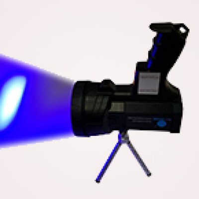
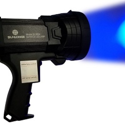
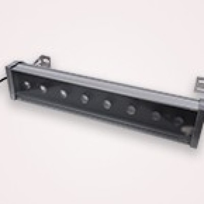
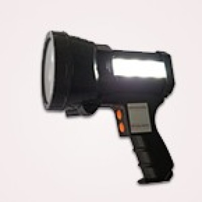
Key Product Example
The Sunlonge SL8100 wafer inspection lamp provides up to 400,000 lux at 30cm, with core parallel light technology, enabling effective detection of even minute defects on large wafers.
Why Is UV Lighting Essential for Wafer Inspection?

- Enhanced Sensitivity: UV light can reveal particles and residue invisible to the human eye or standard visible lighting.
- Non-Destructive: UV inspection is entirely contact-free, ensuring no damage or contamination to wafers during analysis.
- Speed and Throughput: High-intensity LEDs allow fast scanning of entire wafers, minimizing bottlenecks in high-volume manufacturing.
- Detection of Micro-Defects: Enables detection of particles as small as 1μm, cracks, surface scratches, and organic contaminants that could cause chip failures.
Market Impact and Industry Statistics
| Metric | 2025 Expected Value | Significance |
| Global Wafer Inspection Market Size | $4.9B | Rapid growth reflects rising quality demands |
| Semiconductor Defect Inspection Equipment Market | $30.16B | Indicates massive investment in defect detection tech |
| Optical Inspection Share | 57.3% | Optical (including UV) methods dominate for speed/precision |
| Random Defects Revenue Share | 54.6% | Most critical defect type for yield loss prevention |
| Potential Yield Boost Due to Better Defect Detection | Up to 20% | Higher accuracy means significant cost savings |
| TSMC Reduction in Defect Rates via AI/UV Systems | 40% | Industry leaders use advanced detection to slash defects |
How Do UV Wafer Inspection Lamps Improve Defect Detection?
- Fluorescence Detection: Contaminant particles or residues often fluoresce under UV light, “glowing” against the otherwise dark or uniform background of a clean wafer.
- Surface Contrast: UV light exploits differences in material response, making cracks, scratches, and particle defects highly visible compared to visible lighting.
- Real-Time, Inline Inspection: Modern lamps, such as Sunlonge’s SL8100, provide intense, adjustable UV for continuous, inline monitoring vital for large-volume fabs.
Types of Defects Easily Identified
- Particles: Dust, metal contamination, or photoresist residues.
- Cracks: Sub-micron fractures or edge chipping invisible to visible light.
- Organic Residue: Unreacted chemicals or cleaning byproducts.
- Scratches and Surface Voids: Mechanical damage from handling or process deviations.
Q&A: UV Wafer Inspection Lamps
Q1: What advantages do UV wafer inspection lamps have over traditional inspection lighting?
A: UV inspection lamps reveal a broader range of defects, including organic and inorganic contaminants, with higher contrast and sensitivity. They provide non-contact, non-destructive analysis and fast inspection speeds crucial for high-volume semiconductor manufacturing.
Q2: How does UV intensity affect detection capability?
A: Higher UV intensity, such as 400,000 lux at 30cm offered by the Sunlonge SL8100, ensures that even minute particles and surface irregularities are illuminated and visible, allowing consistent detection across large wafers and at higher inspection speeds.
Q3: What is the impact on manufacturing yield?
A: Improved UV-based detection cuts down undetected defects, translating to higher yields, fewer failures, and reduced waste. Leading-edge fabs have recorded yield improvements of up to 20% and defect rate reductions of up to 40% after adopting advanced inspection tools.
Q4: Do UV wafer inspection lamps comply with industry standards?
A: Yes, high-quality lamps—such as those from Sunlonge—adhere to standards like ASTM E3022, ensuring reliability and acceptance for use in regulated industries (aerospace, automotive, electronics).
Comparison Table: Key Features of UV Wafer Inspection Lamps
| Feature | Sunlonge SL8100 Wafer Inspection Lamp | Industry Standard |
| UV Intensity | 150,000 – 400,000 lux at 30cm | 20,000 – 40,000 lux typical |
| UV Wavelength | 365nm (Optimized for fluorescence) | 365-370nm |
| Inspection Area | Wide, adjustable parallel beam | Fixed/blended |
| Defect Size Detected | <1μm | 1-10μm |
| Compliance | ASTM E3022, RRES 90061 | Varies |
| Portability | Yes (Handheld, adjustable focus) | Often fixed |
| LED Lifetime | >30,000 hours | 20,000+ hours |
Best Practices for Implementing UV Wafer Inspection Lamps
- Select High-Intensity, Uniform Illumination: Ensure the lamp can evenly illuminate the entire wafer at high lux, like the SL8100’s 400,000 lux output.
- Match Wavelength to Application: 365nm is optimal for general residue and defect fluorescence.
- Maintain Clean Lenses and Regular Calibration: Regular checks improve detection accuracy and lamp lifespan.
- Integrate with Automated Systems: Pair lamps with image processing and AI analytics for real-time, inline wafer inspection and feedback.
- Meet Compliance Requirements: Use certified equipment for critical applications, especially in safety or mission-critical chip production.
Conclusion

UV wafer inspection lamps are indispensable for modern semiconductor manufacturing. Their ability to detect sub-micron defects, boost yields, and speed up production has made them a standard in leading-edge fabs worldwide. With advanced products like the Sunlonge SL8100, manufacturers are better equipped to ensure flawless performance and reliability in every wafer—an imperative as chip architectures get ever more complex and the demand for perfect devices rises.