CN
CN
Semiconductor wafer inspection application and visible inspection lamp
Wafer inspection, the technology of detecting defects on a wafer, is a complicated, multistage process in the semiconductor industry. Today we will outline the basics of the inspection process, and how wafer inspection lamp can help during the inspection process.
Fundamentally, wafer inspection is split into 2 categories: patterned wafers and un-patterned wafers. Generally, patterned inspection looks at defeats on processed wafers now containing circuitry. Un-patterned inspection looks at defeats on bare wafers.We will introduce the un-patterned wafer inspection and how wafer inspection lamp should be used in this process.

Un-patterned or bare wafers come in many types of material depending on the application needs. Each wafer has its own specific characteristics. The most common wafer materials are Silicon, Gallium and Silicon Caride (SIC). For example, SIC is widely used in power semiconductor and often focused in application areas such as the automotive industry.
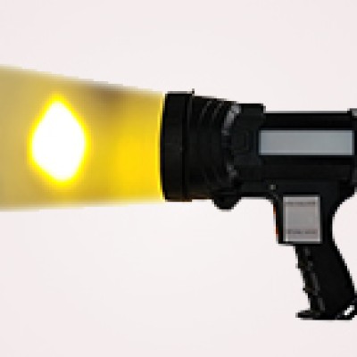
Each of these bare wafer types have inspection needs since defects can come about even in this early stage in the semiconductor fabrication process. The particles may have taken place during the cutting process. The scratches can take place during the polishing process or handling. Both particle and scratches are difficult to detect if with the conventional method. The regular LED is impossible to detect the small size particle and scratches on the pure wafer surface. Wafer inspection lamp is the very tool to locate and identify the common defects.

The light source from the inspection lamp reflects the light on the wafer sample directly. The light source with special color temperature will be diffuse reflection on the sample surface. Then the inspector can detect and locate the defects on the sample surface, eg scratches, particle, dust and so on. This is the basic principle of wafer inspection lamp. Now the wafer inspection lamp with newest technology can detect the defects at minimal 1um size on the sample surface.
In this field, Sunlonge, as the leading manufacturer of wafer inspection lamp, developed the full set of series for customer selection. From the entry model SL8804 to the high end SL8100 model, we got different lamps for customers with different demand.